中文
中文

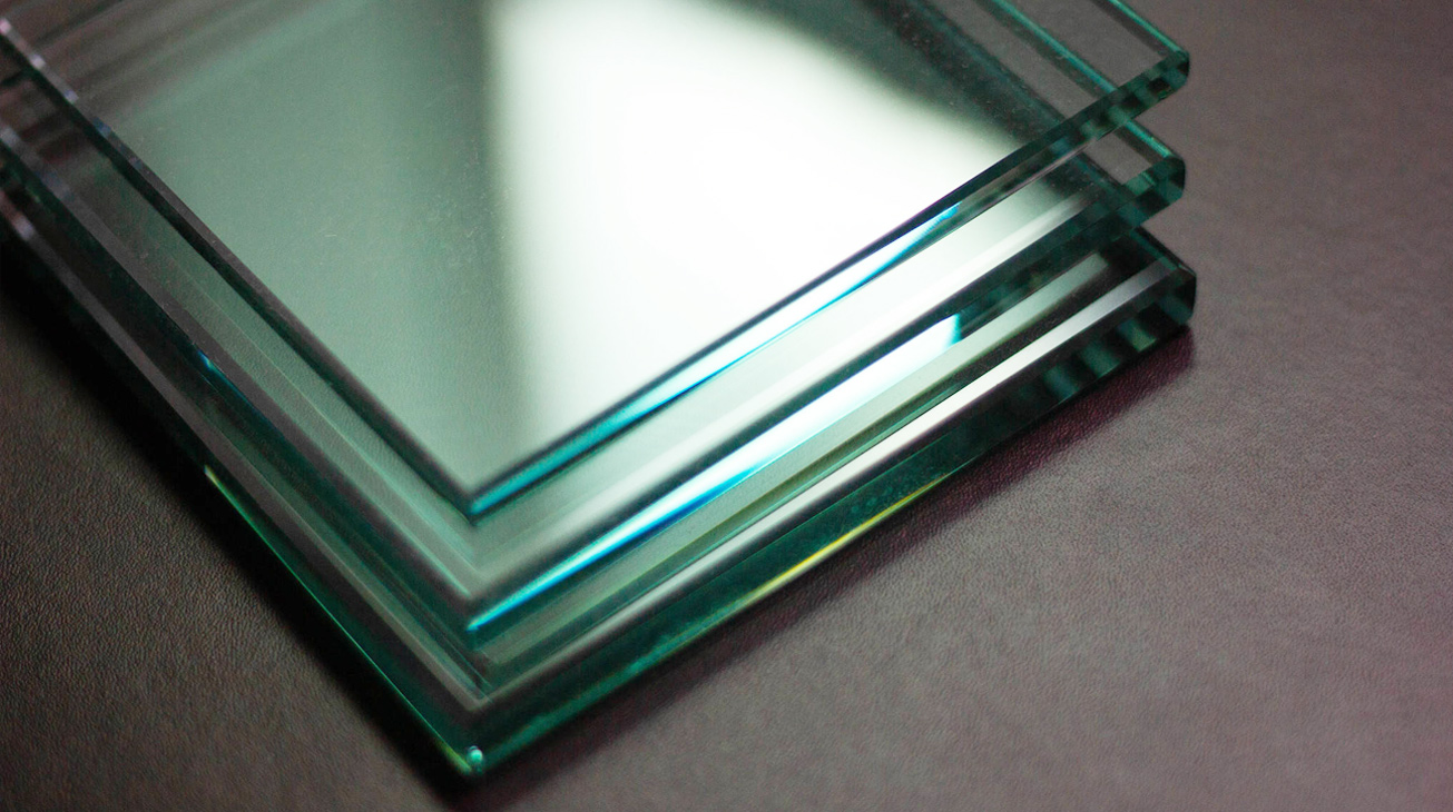
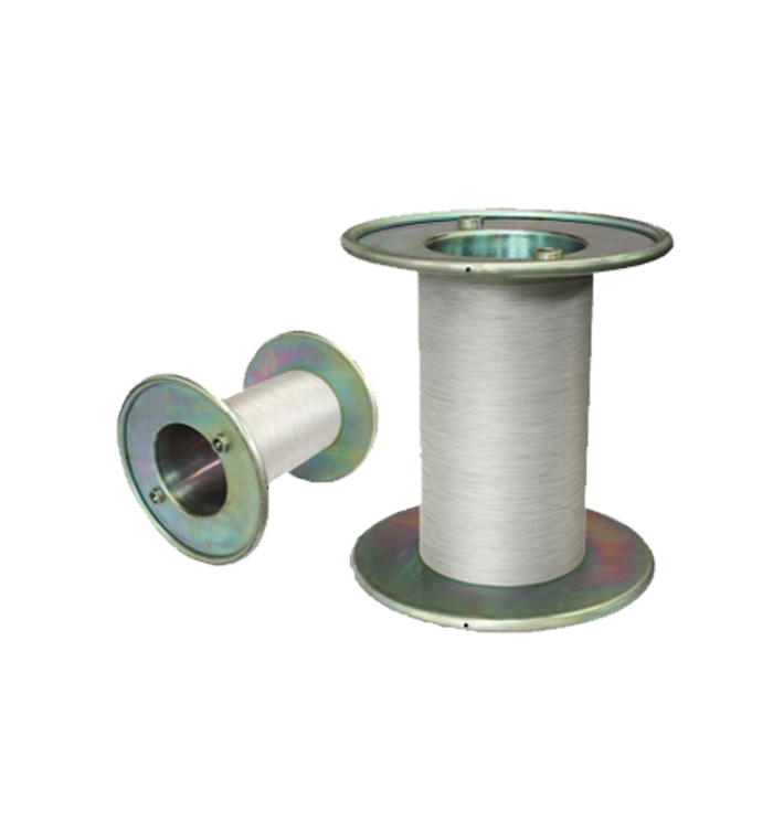
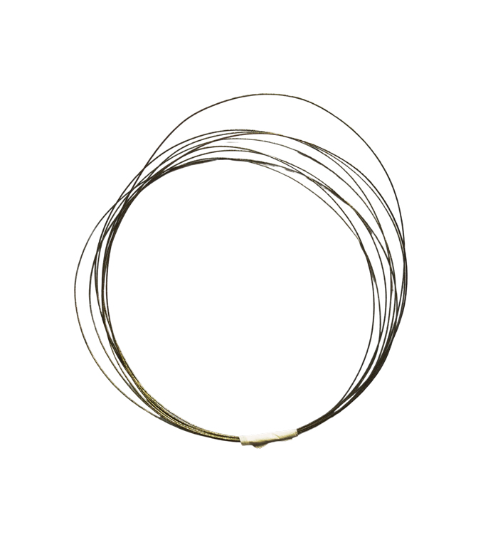
Diamond wire is the core tool for precision cutting of hard and brittle substrate materials such as silicon wafers, silicon carbide (SiC), and gallium nitride (GaN) in the semiconductor industry. It directly determines the accuracy, yield, and cost of substrate processing and is a key support for the "front-end material processing" of semiconductor manufacturing. Its core application scenarios and technological value are as follows:
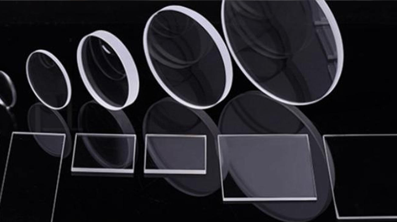
Silicon wafer cutting: used for "square slicing" processing of 8-12 inch (mainstream size) silicon single crystal ingots, reducing silicon material loss and adapting to the strict requirements of logic chips and storage chips for wafer flatness.
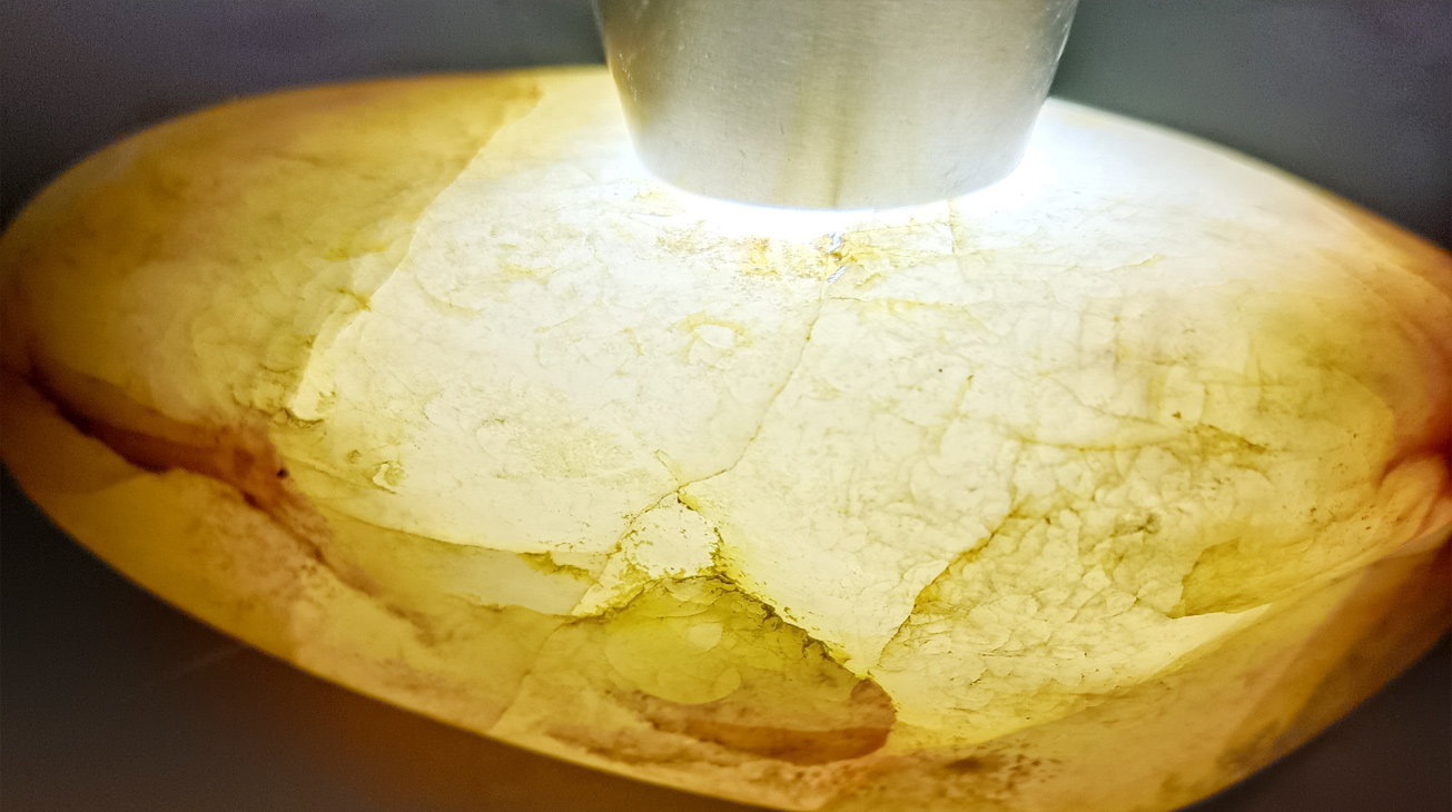
Third generation semiconductor substrate cutting: Targeting substrates with higher hardness (Mohs hardness 9.5+) such as silicon carbide and gallium nitride, it can solve the problem of traditional cutting "edge breakage and cracking", especially suitable for slicing and cutting 2-6 inch silicon carbide substrates, ensuring substrate surface roughness and meeting the high-frequency and high-temperature application requirements of power devices.
Wafer cutting: Before chip packaging, the completed photolithography wafer is cut into independent chips, and diamond lines can achieve "narrow cut" cutting, increasing the number of chips produced per unit wafer.
Low damage processing: There is no mechanical stress concentration during the cutting process, which can avoid internal microcracks in the substrate and significantly improve the yield of subsequent chip manufacturing (such as epitaxial growth and ion implantation), especially for the protection of third-generation semiconductor "high-value substrates" (single silicon carbide substrates cost thousands of yuan).
Product Specifications
Specification Model | Finished product line diameter(μm) | Breaking force(N) | purpose |
45μm | 62±3 | ≥9 | Silicon semiconductor slicing |
65μm | 77±3 | ≥15 | Silicon semiconductor slicing |
70μm | 80±3 | ≥17 | Silicon semiconductor slicing |
100μm | 111±3 | ≥29 | Silicon semiconductor slicing |
*Custom development and manufacturing can be tailored to processing and usage requirements


 ICP:湘ICP备2025139849号-1